Product Description
ILS Flyer
Inscope Labs is a subsidiary of the Semicaps Corporation Pvt. Ltd. It was incorporated in July 2001 to provide prompt, reliable and cost effective analytical services for the semiconductor and disk drive industries. The move to establish a technical support centre equipped with the latest instrumentation and highly experienced application support engineers has received overwhelming positive response from our customers.
To date, more than 5 million Singapore dollars has been invested in the state-of-the-art analytical instruments. Inscope Labs has equipped itself for optical fault localization using Scanning Optical Microscopy (SOM) and Photon Emission Microscopy (PEM); material analysis using Field Emission Scanning Electron Microscopy (FESEM) with Energy Dispersive Spectroscopy (EDS) and Transmission Electron Microscopy (TEM); surface analysis using Field Emission Auger Electron Spectroscopy (AES), X-ray Photelectron Spectroscopy (XPS) and Time-of-Flight Secondary lon Mass Spectroscopy (TOFSIMS); precision TEM and SEM sample preparation using Focus Ion Beam (FIB) techniques and many more.
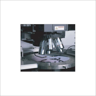
Scanning Optical Microscopy
Scanning Optical Microscopy is applying laser induced phenomena for fault localization on integrated circuits. The system is an integrated system designed for maximum ease of use and flexibility. It is optimized for high laser power delivery, high sensitivity and high spatial resolution.
Photon Emission Microscopy
Photon Emission Microscopy is well known non-destructive method of localizing failure site in semiconductor devices caused by latch-up, contact-spiking, weak oxdles, hot electrons, leaky junctions and other current leakage phenomena.
Electron Microscopy
The field Emission Scanning Electron Microscopy is an ultra high resolution scanning electron microscope for sample observation. Its key feature is the high resolution low eccelerating voltage imaging which is used mainly for Disk Drives and Semiconductor Industries to reduce charging on specimen without coating. Application includes elemental microanalysis.
Auger Electron Spectroscopy
High energy resolution Auger spectroscopy is achieved on the Microlab using a hemispherical sector analyser. This analyser gives the instrument a unique capability to provide precise peak detection and identification including unambiguous chemical state information. Such high energy resolution enables chemical state mapping to be performed on the instrument.
Sample Preparation Equipment
- Decapsulator
- Polisher
- Sputter Coater
- Diamond Saw